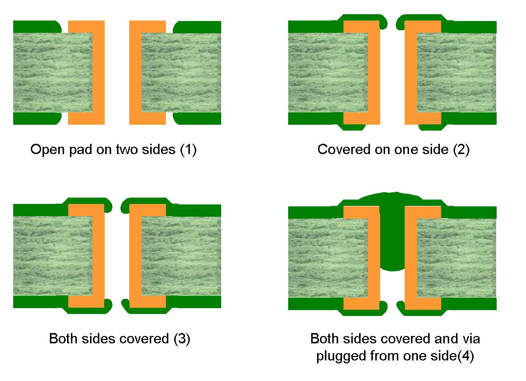
Solder mask and via holes.
Via-hole with no solder mask can cause assembly and reliability problems. When via holes are left open for test purposes there is potential for shorts between pcb and SMT components, especially under BGA’s. Vacuum test fixtures require via holes sealed, either by “via fill” material or by excess solder mask for small vias, but only from one side to avoid air trapping as in image 4 below. For in-circuit-test add test pads to design.
 Solder mask covering types
Standard solder mask (sm) openings are larger than copper pads. For fine pitch, sm openings smaller than copper pads can be used: “Solder Mask Defined Pads” .
Solder mask defined pads are suitable for fine pitch components, often used with BGAs. The solder mask covers the pcb area between adjacent pads and overlaps on top on pad edges. Example below: 20 mil pitch, 4 mil copper pad spacing and 2 mil nominal overlap of solder mask on each pad edge. In images below red is bare pcb and green is solder mask over copper. Solder area can be kept same.
 Standard solder mask opening