Printed Electronics

All of us who have visited a PCB manufacturer knows that it requires a lot of equipment and processes to produce advanced PCBs. In reality, it is worse than it looks. To produce a multilayer pcb about 50 process- steps are required which may involve up to 100 more or less toxic chemicals, lots of electricity and (rinse-) water. PCB manufacturers must invest in advanced air and water treatment plants not to pollute the environment, and a lot of process materials are used and scrapped like drill entry and backing material, multi-layer kraft paper and the etch removal of often most of the copper that was on the laminate when bought! On top of that, a significant part of every production panel become waste materials with high content of mixed metals that does not make it easy to recycle.
Is there any way out of this really environmentally unfriendly materials wastage? The answer is currently no, but a solution for the future may be just around the corner which means that it is time for electronics designers to begin familiarization with a new variant of old technology known as “Printed Electronics “.
“Printed Electronics” is the production of electronic components and/or component carriers using conductive and non-conductive inks by means of printing technology. So far mainly used to produce electronic components in large volumes, typically of flexible materials. The advantage compared to traditional photo patterning by plating and etching is highly efficient material usage as material is applied only where needed without processes to remove what is not required with chemicals or other processes.
The technique also has it’s own umbrella in the organisation called IDTechex http://www.idtechex.com/printed-electronics-europe/pe.asp
As early as the 1980s conductive ink was used instead of copper conductor on PCBs. These were for the most part screened on flexible material and usage was limited to low cost consumer goods. Long thereafter the technology has been reborn and is now used for products like flat screen monitors, credit cards, identification and pricing systems.
A weakness of inks used today is conductivity but with electronic system becomes less energy intensive more products are able to use the technology. Main driver is of course total cost, which is often reduced to a fraction of the cost of traditional technology.
Screen printing has been the most common technique for printing patterns, but it involves a lot of auxiliary equipment like film plotter, developer for film production, exposure equipment for screen stencils, wet- and dark- rooms for developing and setting up and cleaning screens, screen printing machine, oven drying, chemicals, electricity and water. Screen printing is also a limitation in terms of resolution versus yield.
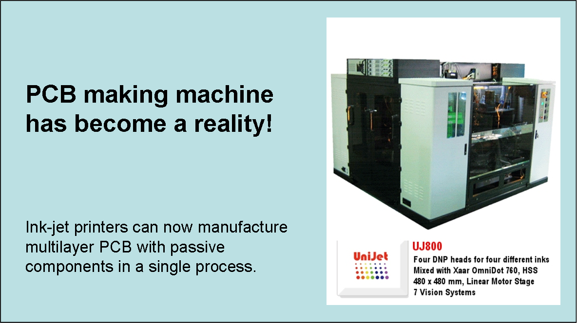
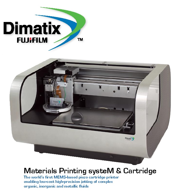
What now is changing this is the introduction of special ink-jet machines that allows layout files to be printed direct from CAD data without additional consumption of materials required before and after, with minimal energy consumption, minimal set–up times and higher resolution!
This opens up a whole new world of possibilities, like building multi-layers with passive components in a single process and connecting layer to layer through strategic overlapping instead of drilled and plated via holes.
Sounds too good to be true, but not with a special ink-jet that can handle several inks in same set-up:
Silver-ink for tracks and pads, gold-ink for contacts, carbon ink for resistors and a dielectric ink for isolation layer to layer and between small gaps between tracks. The very thin dielectric layers also provide possibilities to add capacitance areas, which also can be stacks or multilayer capacitors! Connections through substrate can be done by making small holes prior to applying ink over smd in them on one side, then make matching traces on opposite side, and connection is complete. See Figure
The Japanese are as usual early ahead in new technologies and Epson have received state aid to research new Ink-Jet printer capabilities. Currently they have succeeded to produce 20-layer pcbs with applications in information and communication technology.
But can soldering be used in the new processes? Not yet and probably not. What looks more feasible is to have an assembly machine that applies conductive pastes followed by component placement in the wet ink before drying.

