PCB Build Illustrations
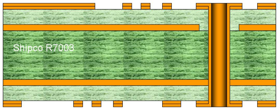
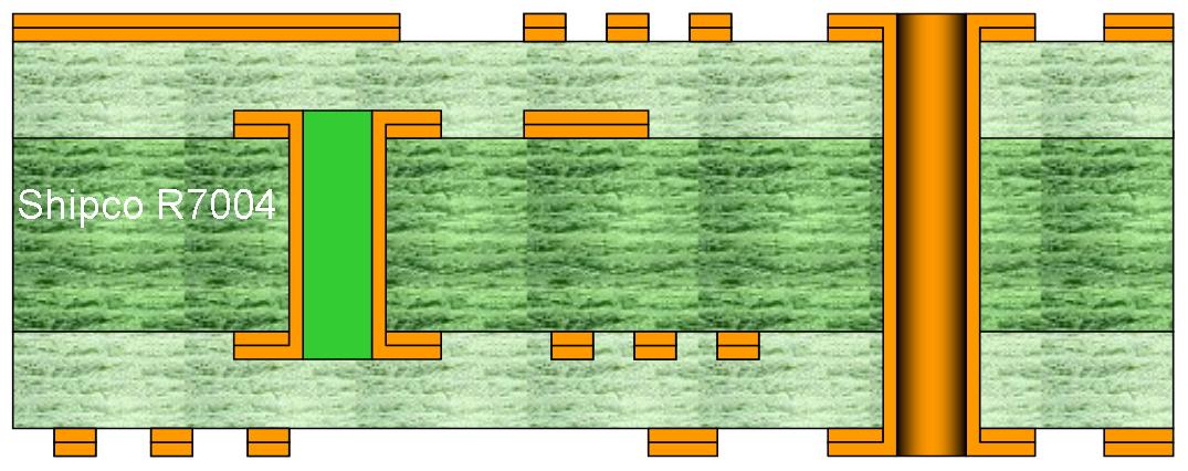
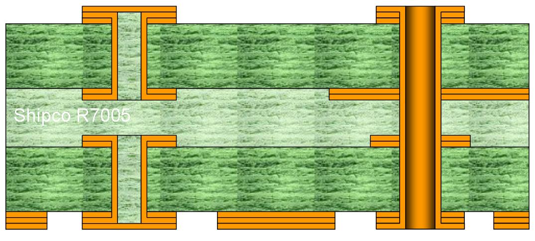
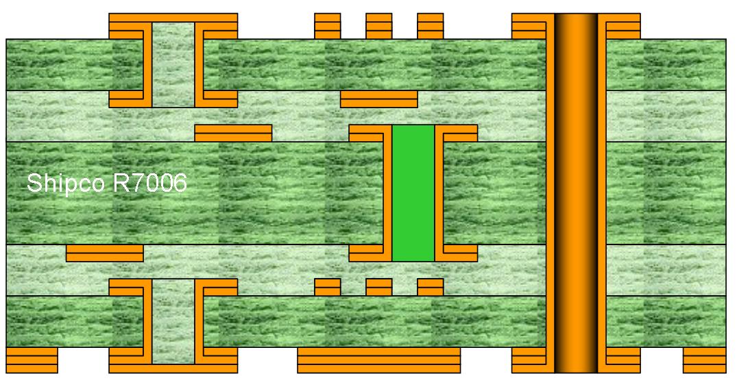
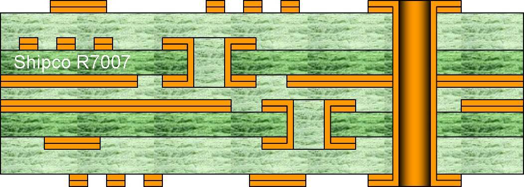
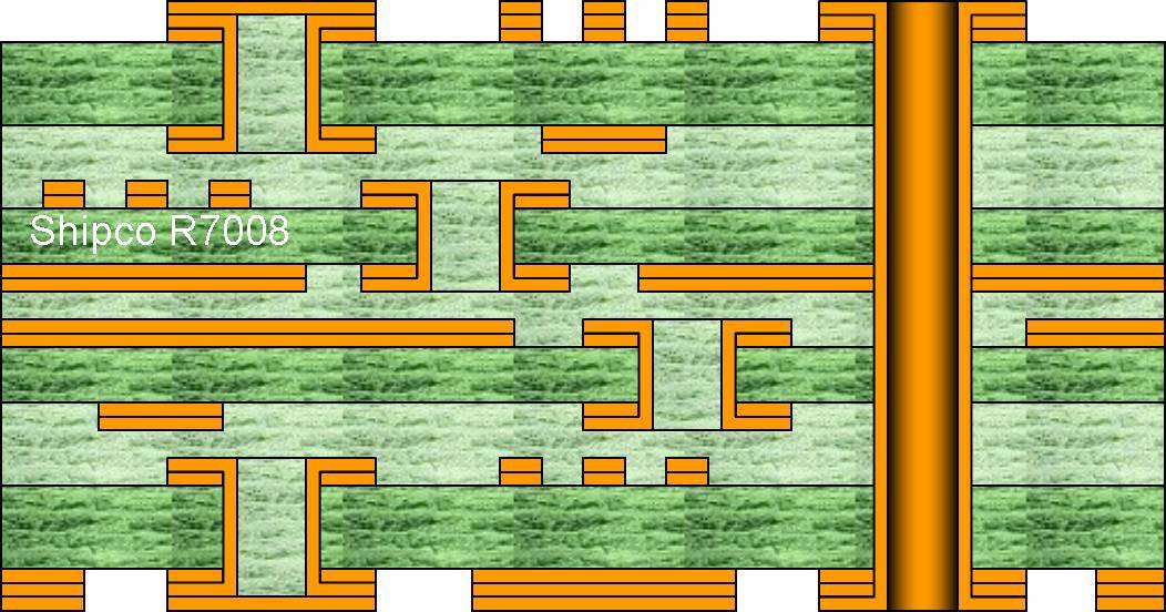
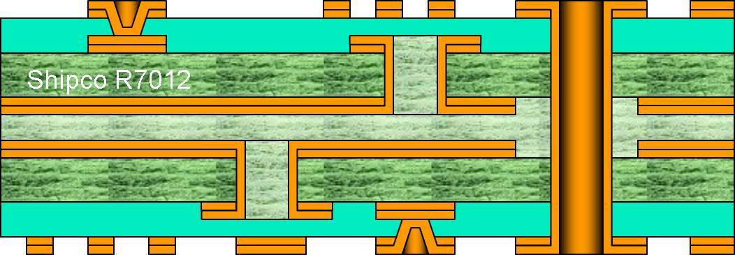
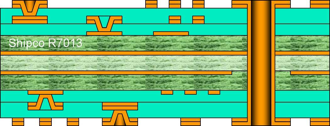
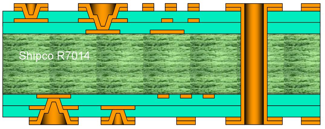
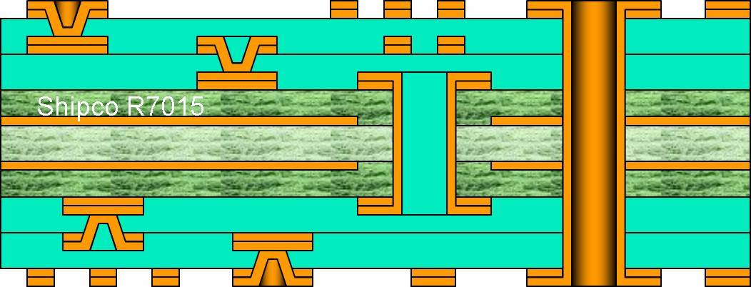
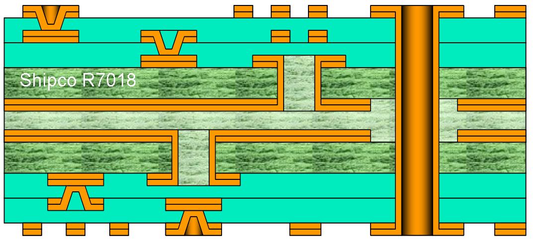
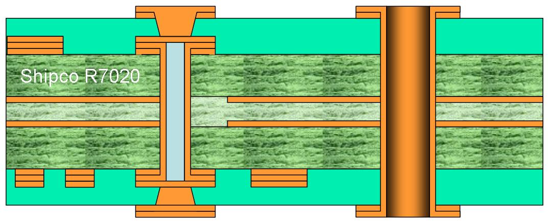
Our PCB build illustration diagrams show common PCB builds. Browse the selection of PCB construct methods below. There are many ways to build a board but the ones listed are industrially sound and commonly used. This is a useful framework based on years of industrial experience, showing methods that are tested and proven to work. If you want more information about a specific build please send us an email!
Routing constraints in a layout can easily be solved by increasing build complexity, like adding another layer or blind and buried vias. The pcb cost can increase rapidly using complex builds with more layers, maybe buried and blind vias, laser vias, flexible pcb, flex-rigid etc., and also mean longer lead times and fewer able suppliers, but most of the options are below. Builds must also be symmetric or no serious supplier can manufacture boards without warp.
Symmetric build means new layers added symmetrically at both sides at same stage, thicknesses of added layers near same, copper planes near same thickness and close to same overall areas, and placed symmetrically. Most build examples are shown as 4 or 6 layers yet number of layers is usually not a limitation.
Finally don’t forget that the “art” in pcb layout is to fit complex circuitry into simple builds. The graphics on this page are totally free to copy for private, educational or commercial purposes! Right-click – “copy image” – and paste in email or anywhere. Image size can typically be adjusted after pasting.
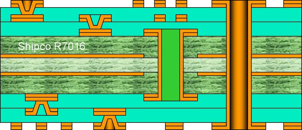
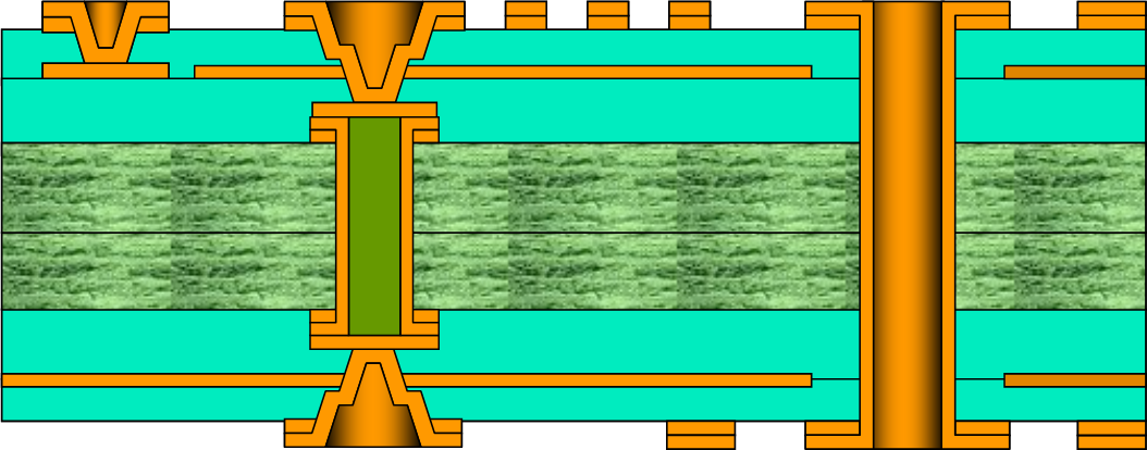
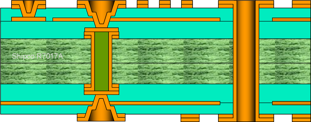
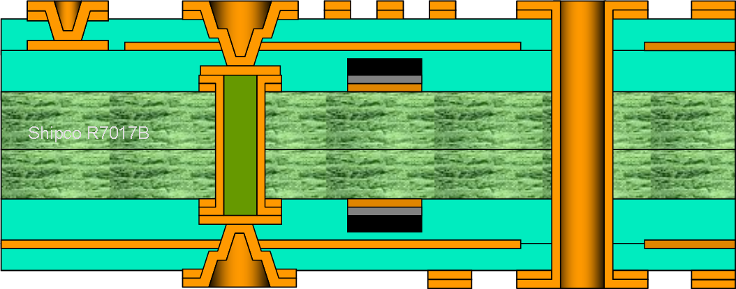
Illustrations have unique numbers, such as: R700xx. These numbers provides references to these builds and the references can typically be found in web searches.
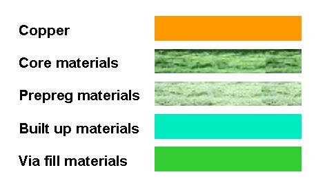

Double sided PCB illustrations


Micro via builds – R7009


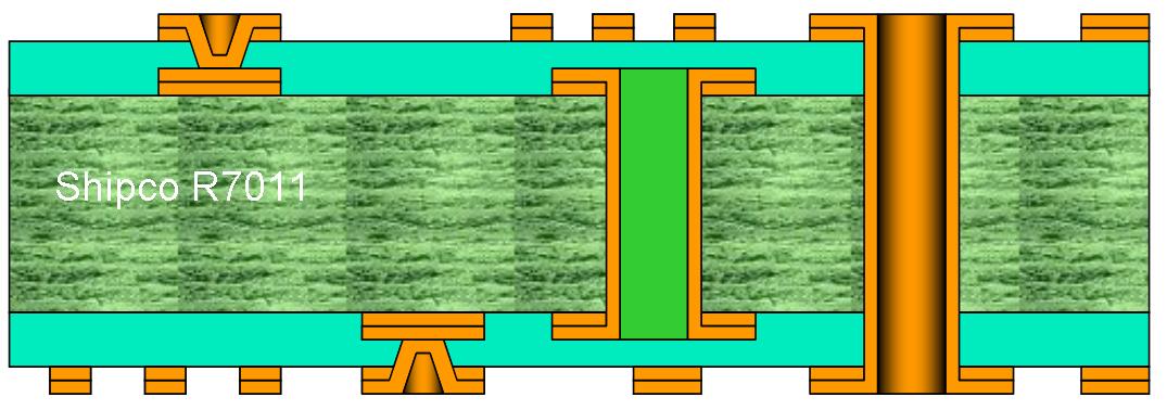

Flex and Flex Rigid start at R7021


